
PCB Factory
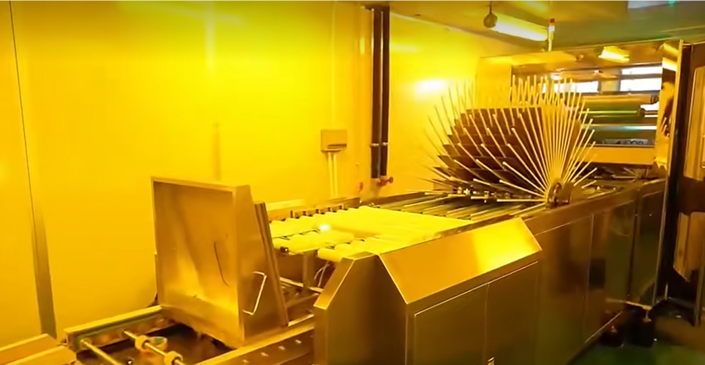
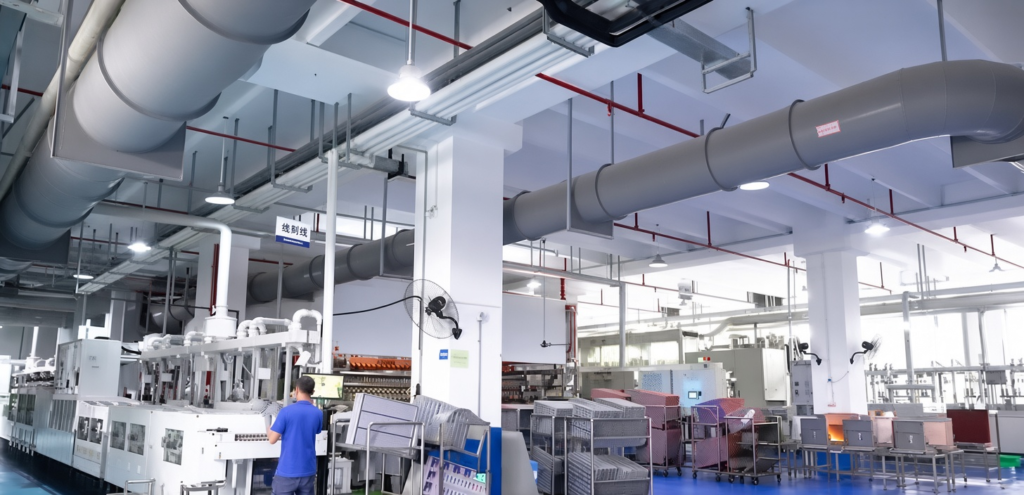
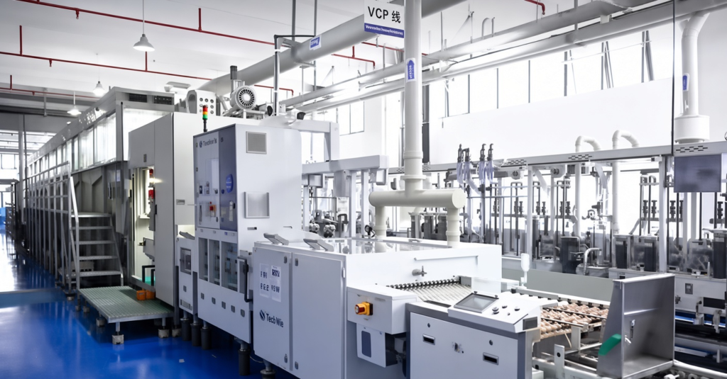
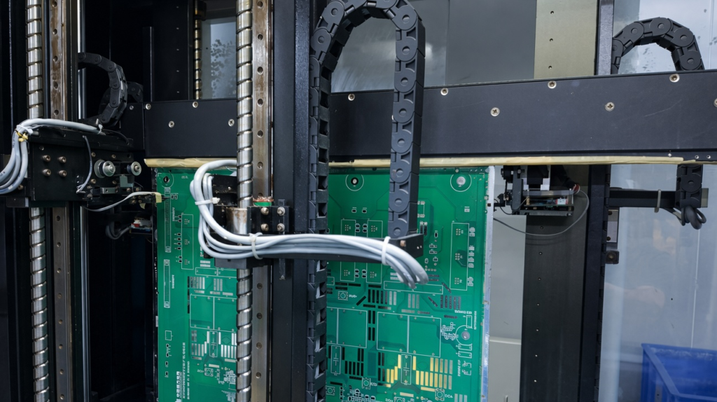
We provide PCB fabrication for prototypes and production orders, with engineering support to review your manufacturing files and project requirements. Share your Gerber files, specifications and required quantities with us to request a quote.
PCB Types
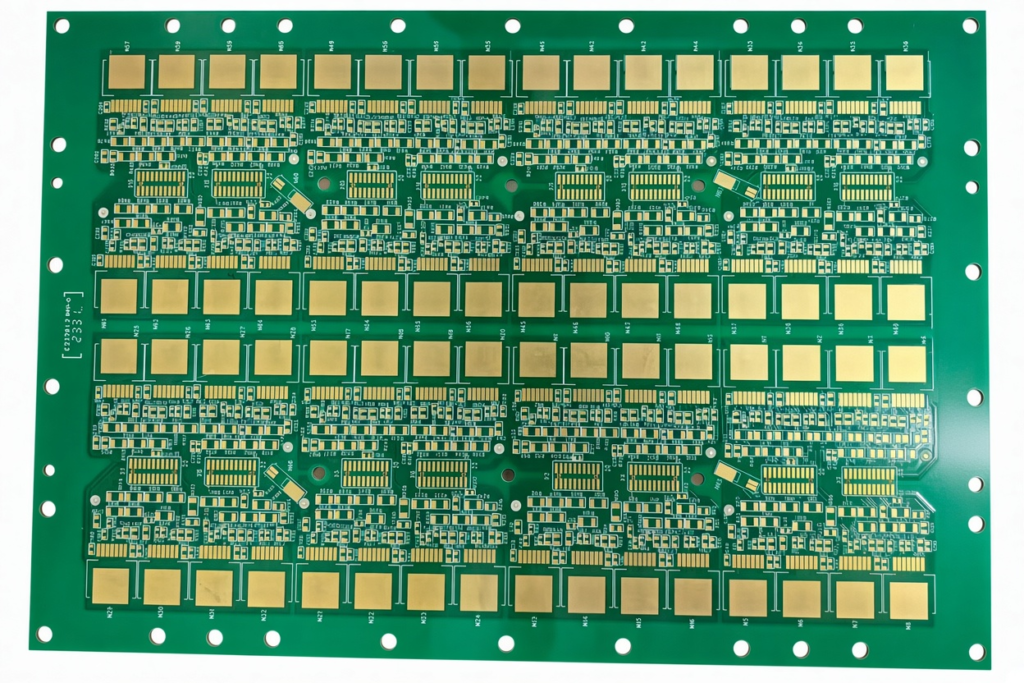
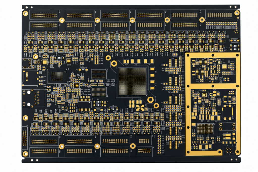
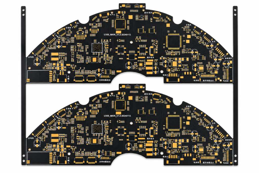
- Single-Sided, Double-Sided & Multilayer PCBs
- HDI PCBs with Blind & Buried Vias
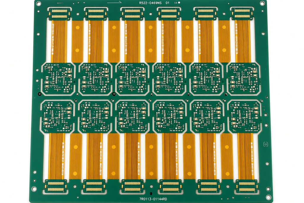
- Flexible & Rigid-Flex PCBs
- Aluminum PCBs
- High-Frequency PCBs
- Castellated (Half-Hole) PCBs
PCB Manufacturing Capabilities
Use the specifications below as a starting point for your PCB project. Send your fabrication files and material requirements so we can confirm the manufacturing options for your design.
Board Structures & Materials
| Specification | Available Options |
|---|---|
| Layer Range | Standard fabrication: 1–20 layers. Higher layer counts require a review of your design files. |
| Board Structures | Rigid, HDI, flexible, rigid-flex, aluminum-backed and high-frequency PCBs |
| Substrate Options | FR-4, high-Tg FR-4, halogen-free FR-4, polyimide, aluminum and PTFE |
| RF & High-Frequency Laminates | Rogers, Taconic, Nelco and Arlon. Specify the required grade when requesting a quote; availability will be confirmed. |
| Finished Board Thickness | 0.1–10.0 mm |
| Copper Weight | 0.5–6 oz. For pilot runs requiring 12 oz copper, submit your files for technical review. |
Feature Sizes & Tolerances
| Specification | Manufacturing Capability |
|---|---|
| Minimum Trace Width / Spacing | 0.075 / 0.075 mm (3 / 3 mil) |
| Minimum Mechanically Drilled Hole | 0.10 mm |
| Minimum Laser-Drilled Hole | 0.075 mm |
| Outline Accuracy | ±0.10 mm |
| Trace Width Tolerance | ±10% |
| Hole Position Accuracy | ±0.05 mm |
| Hole Diameter Tolerance | Plated holes (PTH): ±0.076 mm; non-plated holes (NPTH): ±0.05 mm |
| Minimum Solder Mask Bridge | 0.05 mm |
| Controlled Impedance Tolerance | ±8% |
Surface Finishes & Special Processes
| Process | Available Options |
|---|---|
| Solderable Surface Finishes | HASL, lead-free HASL, ENIG, immersion tin, immersion silver, OSP and ENEPIG |
| Additional Surface Processes | Gold plating, gold fingers and carbon ink |
| Via & Drilling Processes | Blind vias, buried vias and back drilling |
| Edge & Stack-Up Options | Castellated (half) holes and hybrid stack-ups |
Listed capabilities depend on the combination of material, stack-up and board features. Not all limits apply simultaneously. Your quotation will confirm the agreed specifications and production lead time after technical review.
PCB Production Lead Times
| Layer Count | Expedited Prototypes | Standard Prototypes | Volume Production |
|---|---|---|---|
| 1–2 Layers | 24–48 Hours | 2–5 Days | 5–7 Days |
| 4–8 Layers | 48–72 Hours | 5–7 Days | 7–10 Days |
| 10–18 Layers | 10–15 Days, subject to design review | ||
| Above 20 Layers | 15–20 Days, subject to technical review and manufacturing approval | ||
Days refer to working days. Lead times are indicative and depend on design complexity, material availability and order quantity. Expedited service is subject to confirmation. Final production lead time is confirmed during quotation; shipping time is additional.
Request a PCB Fabrication Quote
Send your Gerber and drill files, required quantity, material, board thickness, copper weight and surface finish. Include your stack-up, impedance requirements and target delivery date where applicable. We will review your files and confirm pricing and lead time.