
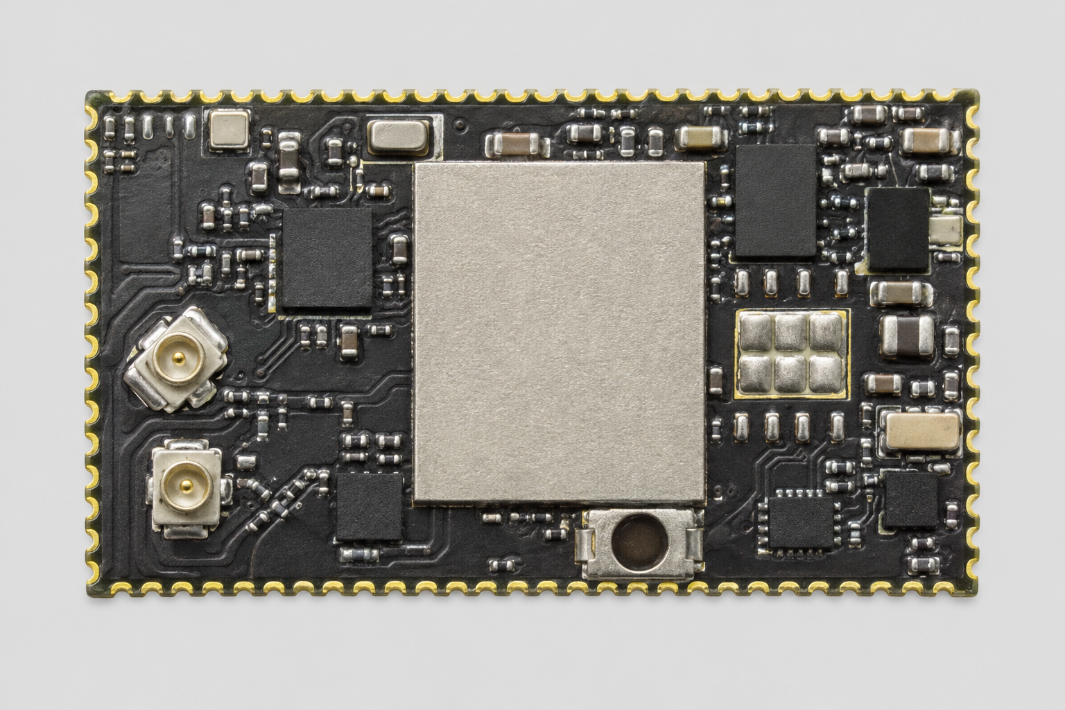
8-Layer HDI RF PCB Assembly for IoT: A 22-Day Prototype Project
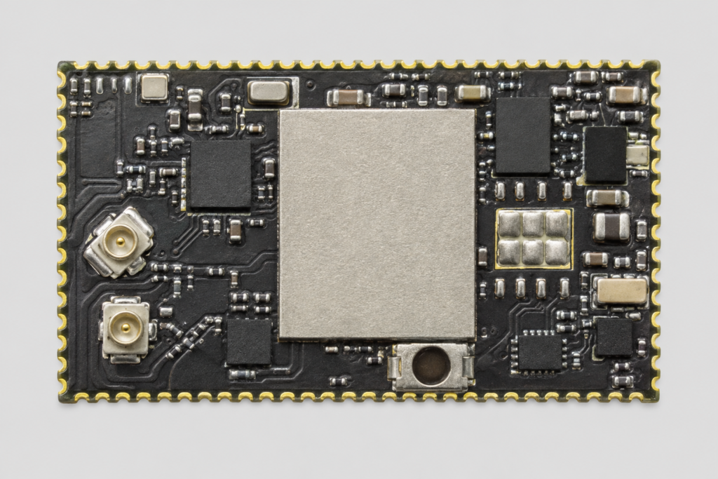
An IoT customer needed an 8-layer, three-stage HDI RF board with BGA components manufactured and assembled for prototype testing. The project required careful manufacturing review and material coordination to meet a tight schedule.
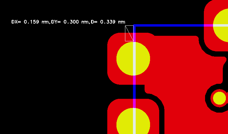
Before production, our team reviewed the PCB files and checked the BOM. This identified two issues that could affect delivery: closely spaced castellated holes and components with long procurement lead times.
| Item | Project Details |
|---|---|
| Application | IoT |
| PCB Structure | 8-layer, three-stage HDI |
| Assembly Features | RF circuitry and BGA components |
| Services | PCB fabrication, component coordination, assembly, programming and testing |
| Total Turnaround | 22 days |
DFM Review Identified a Castellated Hole Risk
Our pre-production DFM review identified closely spaced castellated holes, which increased the risk of hole-edge breakout during PCB fabrication.
Because the customer needed prototypes urgently, the prototype build proceeded with the original design. The spacing recommendation was retained for the subsequent production revision.
For the later volume-production run, the customer increased the castellated hole spacing based on our feedback. This change reduced manufacturing scrap, with estimated savings of US$1,500–2,000 in scrap and replacement production costs and shorten 15 days lead time.
Nitrogen Reflow for the Compact BGA Assembly
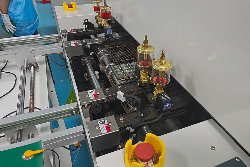
The compact RF board included BGA components, making soldering process control an important part of the prototype build. We used nitrogen reflow soldering to limit oxidation during reflow and support solder wetting. The reflow profile was selected for the assembly requirements.
Customer-Supplied Components Helped Address Long Lead Times
Our BOM review also identified components with long procurement lead times. Waiting for these parts through the original sourcing plan could have delayed the prototype build.
We discussed the available options with the customer, who arranged to supply selected components to us. This allowed the project to proceed without waiting for those parts to be purchased through our sourcing process.
Coordinating customer-supplied parts with PCB fabrication helped keep the assembly schedule on track.
From PCB Fabrication to Completed Assembly in 22 Days
The project was completed in two production stages:
- PCB fabrication: 17 days
- Assembly, programming and testing: 5 days
The total turnaround from PCB fabrication through completed PCBA was 22 days, providing the customer with prototypes for their planned evaluation.
Project Outcome
Early file review and customer coordination helped address manufacturing and material risks before they became production delays.
The project achieved:
- A customer-approved revision to improve castellated hole spacing
- Reduced risk of PCB scrap and replacement manufacturing
- Estimated potential cost avoidance of US$1,500–2,000
- Coordination of customer-supplied, long-lead components
- Completed PCB fabrication and assembly within 22 days
The turnaround and estimated savings relate to this specific project. Results and lead times depend on board complexity, material availability, quantities and testing requirements.
Discuss Your IoT PCB Assembly Project
Planning an RF or HDI PCB assembly prototype? Send your Gerber files, BOM, pick-and-place data, quantities and target schedule. We can review manufacturing requirements and discuss material sourcing options before production.
Email: engineer@trustedpcba.com
WhatsApp: +86 159 8600 8624